

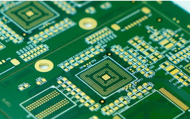
Modern electronic products continue to become smaller, faster, and more powerful, creating new challenges for printed circuit board design and manufacturing. Smartphones, wearable devices, medical equipment, automotive electronics, communication systems, and industrial automation all require compact circuit boards capable of supporting high component density and high-speed signal transmission. Traditional PCB technologies often struggle to meet these demanding design requirements, making the HDI PCB an increasingly popular solution for advanced electronics.
High-Density Interconnect (HDI) PCBs are designed with finer traces, smaller vias, higher connection density, and multiple routing layers that allow engineers to build complex circuits within compact board dimensions. Their advanced structure improves electrical performance while reducing product size, making them ideal for modern high-performance electronic systems.
Because HDI circuit boards require sophisticated manufacturing technologies, laser drilling, sequential lamination, and precision quality control, selecting an experienced HDI PCB manufacturer China has become an important decision for companies seeking reliable production, competitive pricing, and consistent quality.
This article explains what an HDI PCB is, how it is manufactured, its advantages, applications, and why partnering with an experienced manufacturer in China can contribute to successful product development.
What Is an HDI PCB?
An HDI PCB is a high-density printed circuit board designed with advanced interconnection technologies that allow more electrical connections within a smaller physical area than conventional multilayer PCBs. These circuit boards typically feature fine-line copper traces, microvias, blind vias, buried vias, and multiple sequentially laminated layers to maximize routing efficiency.
Unlike traditional circuit boards, HDI PCBs provide significantly higher wiring density, allowing engineers to design compact electronic products without sacrificing functionality or electrical performance. The use of laser-drilled microvias enables reliable interconnections between layers while minimizing space requirements.
HDI technology supports increasingly complex integrated circuits, fine-pitch components, ball grid arrays, and high-speed processors commonly used in today’s electronic devices.
As miniaturization continues across nearly every industry, HDI PCBs have become an essential technology for modern electronic product development.
Why HDI PCBs Are Important
The demand for smaller electronic products with greater processing power has made efficient PCB design more important than ever. An HDI PCB enables engineers to integrate more electronic components into compact layouts while maintaining reliable electrical performance.
Higher routing density improves signal transmission by reducing trace lengths and minimizing signal loss. This contributes to better signal integrity, faster communication speeds, and lower electromagnetic interference, all of which are essential for high-frequency electronic applications.
Microvia technology also improves electrical reliability by shortening connection paths between circuit layers, reducing inductance and improving high-speed signal performance.
The compact design of HDI PCBs supports lightweight electronic products while allowing manufacturers to incorporate additional functionality into smaller devices. This makes HDI technology particularly valuable for industries where product size and performance are equally important.
The HDI PCB Manufacturing Process
Manufacturing an HDI PCB begins with a comprehensive Design for Manufacturability (DFM) review. Engineers evaluate layer stack-up, impedance control, trace geometry, microvia structures, material selection, and manufacturing tolerances before production begins.
The fabrication process starts by producing the individual copper layers using precision photolithography and chemical etching. Laser drilling technology creates extremely small microvias that connect adjacent layers with exceptional accuracy.
Sequential lamination techniques gradually build the multilayer PCB by bonding additional dielectric and copper layers while maintaining precise layer alignment. Copper plating forms reliable electrical connections inside the microvias before further imaging and etching create additional routing layers.
Protective solder mask, silkscreen printing, and high-quality surface finishes prepare the completed PCB for component assembly. Throughout manufacturing, advanced inspection technologies verify dimensional accuracy, microvia integrity, and electrical performance before shipment.
The combination of precision manufacturing equipment and carefully controlled production processes is essential for producing reliable HDI circuit boards.
Advantages of HDI PCB Technology
One of the greatest advantages of an HDI PCB is its ability to significantly increase component density while reducing overall circuit board size. Engineers can integrate highly complex electronic systems into compact products without compromising functionality.
Improved signal integrity is another major benefit. Shorter routing paths reduce signal delay, electromagnetic interference, and transmission losses, making HDI PCBs suitable for high-speed digital circuits and communication systems.
The lightweight design contributes to smaller electronic products while supporting improved thermal performance through optimized layer structures and copper distribution.
HDI technology also enhances mechanical reliability because laser-drilled microvias reduce stress concentrations that may occur in traditional mechanically drilled vias during thermal cycling.
These combined advantages make HDI PCBs ideal for products requiring advanced performance, compact dimensions, and dependable long-term reliability.
Applications of HDI PCBs
HDI PCBs are widely used across industries that require high-performance electronics with compact form factors. Consumer electronics manufacturers incorporate HDI technology into smartphones, tablets, laptops, wearable devices, digital cameras, gaming systems, and smart home products.
Automotive manufacturers use HDI PCBs in advanced driver assistance systems, electric vehicle controllers, battery management systems, infotainment platforms, autonomous driving electronics, and engine control units where space and reliability are critical.
Medical equipment manufacturers depend on HDI circuit boards for portable diagnostic devices, patient monitoring systems, imaging equipment, implantable medical electronics, and wearable healthcare products requiring miniature yet reliable circuitry.
Telecommunications infrastructure utilizes HDI PCBs in networking equipment, communication switches, optical transmission systems, base stations, and high-speed communication hardware.
Industrial automation, aerospace electronics, defense systems, robotics, Internet of Things devices, artificial intelligence hardware, and advanced computing platforms also benefit from the superior capabilities of HDI PCB technology.
Why Choose an HDI PCB Manufacturer China?
Working with an experienced HDI PCB manufacturer China offers significant advantages for companies developing advanced electronic products. China has become one of the world’s leading centers for PCB manufacturing, supported by extensive production infrastructure, advanced equipment, and highly skilled engineering teams.
Many Chinese manufacturers operate modern facilities equipped with laser direct imaging systems, laser drilling machines, automated optical inspection, X-ray inspection, flying probe electrical testing, and intelligent manufacturing systems capable of producing highly complex HDI circuit boards.
Experienced manufacturers also provide engineering support during prototype development by performing Design for Manufacturability analysis, stack-up optimization, impedance calculations, and production planning to improve manufacturability and reduce project risks.
In addition to advanced technical capabilities, manufacturers in China often offer competitive production costs, scalable manufacturing capacity, efficient supply chain management, and shorter lead times for both prototype and volume production.
Selecting a reputable manufacturing partner helps ensure consistent product quality while supporting efficient global electronics production.
Quality Assurance in HDI PCB Manufacturing
Quality assurance is especially important in HDI PCB production because of the extremely fine geometries and complex multilayer structures involved. Manufacturers inspect incoming materials before monitoring every production stage using advanced process control systems.
Automated Optical Inspection identifies defects such as open circuits, short circuits, incorrect trace widths, and missing copper features before lamination. X-ray inspection verifies internal layer alignment, plated microvias, and hidden electrical connections throughout the completed PCB.
Electrical testing confirms circuit continuity, insulation resistance, impedance performance, and overall functionality before shipment. Additional reliability evaluations frequently include thermal cycling, solderability testing, dimensional inspection, microsection analysis, and environmental testing to ensure dependable long-term operation.
Leading manufacturers maintain internationally recognized certifications including ISO 9001, IPC standards, UL certification, IATF 16949 for automotive electronics, ISO 13485 for medical devices, and RoHS compliance. These certifications demonstrate their commitment to producing reliable HDI PCBs that meet global quality standards.
Conclusion
The HDI PCB has become a cornerstone of modern electronic product development, enabling manufacturers to create smaller, faster, and more sophisticated devices without sacrificing performance or reliability. Its high-density routing capabilities, superior signal integrity, compact design, and excellent electrical characteristics make it the preferred solution for consumer electronics, automotive systems, telecommunications, healthcare, aerospace, industrial automation, and many other advanced applications.
Partnering with an experienced HDI PCB manufacturer China provides access to advanced manufacturing technologies, engineering expertise, and comprehensive quality assurance processes. As electronic products continue to evolve toward greater complexity and miniaturization, HDI PCB technology will remain essential for developing innovative, reliable, and high-performance electronic solutions for global markets.
